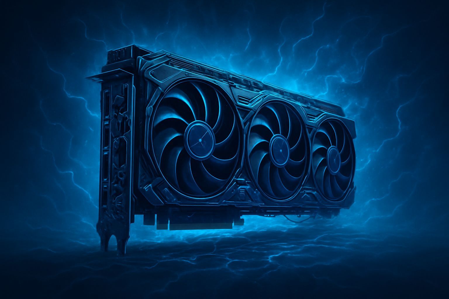
In the vast and constantly evolving panorama of PC hardware, few graphics cards have left such a significant footprint as the AMD Radeon RX 500 series, and in particular the RX 580. Launched in 2017, Radeon RX 580 was not a technological revolution, but rather a refined evolution of Polaris architecture, which debuted with the RX 480. This strategy, typical of AMD at that time, aimed to optimize performance, efficiency and stability, making Polaris GPUs extremely competitive in the mid-range market segment. The Sapphire Nitro+ Radeon RX 580 8GB, the subject of many analyses and reviews at the time, emerged as one of the leading models, gaining the reputation of preferred choice for fans and value-conscious gamers. Its longevity, also complicit in the boom of cryptocurrency mining that has supported its demand for years, testifies to the solidity of its design and its engineering. However, behind marketing specifications and performance numbers, there is a world of complex design decisions, engineering compromises and innovative solutions that deserve a thorough analysis. This article aims to go beyond the simple review, virtually disassembling Sapphire Nitro+ RX 580 to explore its critical systems in detail: from intricate digital power to delicate memory balance, to the ingenious cooling system that allowed this card to maintain high performance under load. Understanding these aspects is not only an exercise of technological curiosity, but also offers a window on the evolution of graphic design and the fundamental principles that guide the development of high-performance hardware, providing a broader perspective on the complexity and ingenuity that characterize every component of our digital ecosystem. The approach of Sapphire with Nitro+, balancing costs and performance with an eye to durability, has created a precedent for future generations of graphics cards, making it an exemplary case study for anyone who wants to understand the true dynamics of GPU engineering.
no
The Art of Digital Food: From Theory to Practice in RX 580
no
The power of a graphics card is a component often underestimated but of crucial importance, since it determines the stability, efficiency and the potential of overclocking of the GPU. In the case of the Sapphire Nitro+ Radeon RX 580, the power circuit architecture, or Voltage Regulator Module (VRM), is a striking example of how marketing specifications can sometimes differ from engineering reality, while offering a robust and effective final result. Sapphire has advertised six feeding stages for the GPU, a number that suggests considerable stability and ability to manage high loads. However, a more thorough analysis of the PCB reveals the use of a PWM ON Semiconductor NCP81022 controller, a chip designed to manage a maximum of 4+1 phases. The discrepancy is resolved through a technique known as phase doubling (phase doubling). This solution employs a trio of NCP81162 phase duplicators mounted on the back of the board, which double the output of the three actual phases managed by the main controller, creating six voltage regulation circuits working in parallel. Although it is not six phases *native* and completely independent, doubling still offers significant benefits in terms of load distribution and stress reduction on individual components. Each power channel, in this case you are, uses an integrated power station Vishay SiC632. These advanced chips combine high-side and low-side MOSFETs into a single package, a gate driver and a Schottky diode, improving efficiency and reducing space occupied on the PCB. Theoretically, each SiC632 can handle up to 50A, although the practical value is slightly lower. This configuration, although efficient, still generates significant heat: it is estimated a power loss from 6 to 8 watts per stage, for a total of about 50 watts of heat to be dissipated only by the VRM of the GPU. The presence of three 10A fuses for the GPU and one for the memory offers essential protection, limiting the maximum output to 360 watts for the GPU, more than enough for Ellesmere, and ensuring the safety of the card, even if a burnt fuse still requires a guarantee. Voltage monitoring is entrusted to a TI INA3221, which provides precise data for energy management. As for memory power, the solution is simpler, controlled by a synchronous buck converter Anpec APW8722 and composed of a MOSFET N-channel ON Semiconductor NTMFS4C10N on the high side and two on the low side, powered directly by the PCIe slot. This complex yet well implemented architecture demonstrates the ingenuity required to supply a modern GPU in a stable and reliable way, balancing costs, performance and the need to manage the heat generated, a balance that allowed the Nitro+ RX 580 to excel in its category.
no
Beyond the Frequency: The Crucial Role of Memory Video (VRAM)
no
Video memory, or VRAM, is as vital as the GPU itself, acting as a bridge between the graphic processor and the data it has to process to generate images. The choice of the type, quantity and frequency of VRAM has a direct impact on the overall performance of the graphics card, especially in high resolution gaming scenarios or with very detailed textures. The Sapphire Nitro+ Radeon RX 580 is equipped with 8 GB of SK Hynix memory, specifically H5GQ8H24MJR modules, organized in 32x 256 Mbit. These GDDR5 modules, which at the time represented the state of art for medium and high-end cards, are designed to operate up to 1,55 V and reach a maximum frequency of 2000 MHz, translating into 8 Gb/s of actual throughput. This speed was, for the time, the highest offer from SK Hynix for GDDR5 memory, a detail that, if on the one hand guaranteed solid performance immediately, on the other it suggested a limited overclock margin. Unlike the RX 480, where memory offered a certain potential of tweaking, on the RX 580 of Sapphire the possibilities to further push the frequencies of VRAM were reduced. This is because the chips had already been optimized to operate at the top of their factory specifications. The amount of 8 GB was, and in some ways is still, a significant strength for the RX 580, providing ample capacity to manage the high-resolution textures of modern games and allowing for greater longevity of the board in more challenging contexts. The difference between a 4GB and an 8GB version was already remarkable in some titles, and with time it became even more marked. The power of memory, as mentioned above, is managed by a simpler circuit, but still effective, based on the Anpec APW8722. Although the memory overclocking process did not offer wide margins, the importance of a fast and capacious VRAM cannot be underestimated. The memory bandwidth, determined by the frequency and amplitude of the bus, is a common bottleneck in the graphics cards, and a quick memory allows the GPU to quickly access the necessary data, reducing waiting times and improving the framerate. The evolution from GDDR5 to GDDR5X, then to GDDR6 and finally to technologies like HBM (High Bandwidth Memory) in the most advanced cards, demonstrates the continuous search for solutions to increase bandwidth and memory efficiency, a factor that remains fundamental to unlock the full potential of GPU architectures and meet the increasing demands of the most demanding graphic workloads. The choice of memory for the Nitro+ RX 580 has been a well-studied compromise between cost and performance, which has contributed to the success and lasting popularity of this card in the market.
no
Cold Science: Thermal and Acoustic Design of Graphic Design
no
The cooling system of a graphics card is its Achilles heel or shield, determining not only the ability of GPU to support boost frequencies, but also long-term reliability and user acoustic experience. The Sapphire Nitro+ Radeon RX 580 Limited Edition was designed with a heat sink that had to face at least 250W of dispersed heat, a challenge not recently for a board of that segment. The heart of the cooling system consists of two PWM axial fans produced by Dongguan Champion Electronics. These fans, characterized by a double ball bearing – a choice that increases durability and quietness compared to sleeve bearings – reach speeds between 3250 and 3300 RPM. The rotors, with nine blades and a diameter of 95 mm, were engineered to provide a more diffused air flow rather than concentrated, an approach that aims to cover a wider area of the heat sink evenly. One of the most interesting innovations of Sapphire for Nitro+ was the implementation of a backplate not only aesthetic and protective, but also functional to cooling. Unlike many backplate of the time, which were often thick and inefficient in heat extraction, Sapphire integrated a small aluminum heatsink strategically positioned under the hot points of the PCB, especially in correspondence of phase doubling chips and other VRMs. This heatsink is in direct contact with the backplate through a thin layer of thermal paste, instead of the traditional and less effective thick thermal pads. This configuration greatly improves heat dissipation from the back of the board, which otherwise would accumulate. The main heatsink, 451 grams heavy, incorporates two 8 mm heatpipe and 6 mm, made of nickel-plated composite material. The heatpipes are crushed into a copper base that comes into direct contact with the GPU, ensuring efficient heat transfer. Around the copper base, a light metal plate is responsible for heat transport away from memory modules, while the voltage converters (VRM) have their heatsink integrated into the heatsink itself, a solution that ensures a good part of the air flow intended also to these crucial areas. The heatsink fin design is a well balanced compromise: the density and depth are such as to maximise the surface area without requiring excessive static pressure from the fans, which contributes to reduce the generated noise. Overall, Sapphire's cooling solution on the Nitro+ RX 580 is a mature and optimized design example, which allowed the board to maintain reasonable operating temperatures and a low noise, essential factors for a satisfying user experience and longevity of the card itself, especially at a time when cryptocurre mining pushed GPUs to the limit.
no
The Perfect Balance: Cost, Performance and Duration in GPU Design
no
The design of a graphics card is always the result of a delicate balance between performance, production costs, energy efficiency and durability potential. The Sapphire Nitro+ Radeon RX 580 8GB is an excellent case of study on how a manufacturer can reach a “perfect balance” within the technological and market limitations of its era. The Polaris architecture, of which the RX 580 is the apex, was the result of a continuous optimization of an existing design, focused on the production of an efficient and convenient chip for the mass market. The choice to implement phase doubling in VRM, for example, was a weighted decision: while not offering the purity and independence of native phases, it allowed Sapphire to achieve a power stability and a high current capacity at a lower cost than a completely distinct six-phase design. This compromise resulted in a robust card, capable of sustaining heavy loads and also a discreet overclocking, without making the final price rise too much. Similarly, the adoption of high-speed GDDR5 modules from SK Hynix, while limiting the overclocking margin of VRAM, guaranteed an excellent out-of-the-box bandwidth, sufficient for most 1080p gaming scenarios and even light 1440p. The 8GB of VRAM, in particular, proved to be a far-sighted choice, ensuring the card a longerevity higher than the 4GB models, a crucial aspect in a market where the memory requirements of the games tend to grow constantly. The cooling system, with its double ball bearing fans, the ingenious backplate with integrated heatsink and composite heatpipe, is another example of optimization. Sapphire did not soothe on the materials or complexity of the design where it was necessary, aiming to effectively dissipate the 250W of heat and beyond, while maintaining a contained noise. This attention to thermal management not only improved the immediate performance of the card allowing to support higher boost frequencies, but also significantly contributed to its duration over time, reducing thermal stress on critical components. The presence of a dual BIOS, albeit with more conservative default frequencies, reflected a choice oriented to safety and flexibility, offering users the possibility to choose between a quieter profile or a more performing one, and providing a “paracadute” in case of extreme overclocking. The Radeon RX 580, and in particular the Nitro+ version of Sapphire, has shown that it is not always necessary to reinvent the wheel to create a successful product. The intelligent optimization of an existing architecture, combined with careful hardware engineering and weighted choices on components, can lead to a card that not only offers excellent value for money to launch, but also maintains its relevance and reliability for years, consolidating its status as classic in the GPU pantheon.
no
The legacy of RX 580: A Lighthouse in the Evolution of GPU Design
no
The detailed analysis of Sapphire Nitro+ Radeon RX 580 8GB is not only a hardware archaeology exercise, but a deep immersion in engineering principles that continue to shape the development of modern graphics cards. This card, although not the last technological frontier, embodies many of the challenges and solutions that engineers face daily in the creation of high-performance hardware. His legacy is demonstrating how design optimization, innovation in details and careful consideration of cost and benefits compromises can create a product of great success and longevity. From the complex feeding system with phase doubling, which allowed to achieve stability and power at a low cost, to the oculated management of VRAM memory, which balanced immediate performance and future durability, every aspect of the Nitro+ RX 580 is a testament to ingeniousness. The cooling system, with its robust fans, composite heatpipe and active backplate, was not only an aesthetic hub, but a fundamental component to ensure that the GPU could operate to the maximum of its capacity without thermal throttling and with an acceptable noise. This holistic approach to design, where each component is integrated into a broader vision of performance and reliability, is what made the RX 580 a pillar for mid-range gamers for years, resisting the introduction of successive generations and maintaining a significant value in the market of use. Its history teaches us that the success of a technological product is not only measured according to the highest specifications or the most revolutionary innovations, but also in the ability of a company to cleverly combine existing technology, new ideas and impeccable execution to meet the needs of the market. The lessons learned from the design of the RX 580 continue to influence current graphics cards, from multi-phase VRMs to hybrid cooling solutions, from the importance of VRAM to advanced energy management. It is a reminder that, even in a future-oriented industry, the thorough understanding of engineering foundations and meticulous detail optimization are the key to building products that not only work, but excel and leave a lasting footprint in the technological ecosystem. The Sapphire Nitro+ Radeon RX 580 remains, therefore, much more than a simple graphics card; it is a symbol of an era and a master example of hardware engineering well realized.


